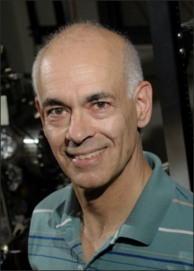
Joseph W. Lyding is the Robert C. MacClinchie Distinguished Professor of Electrical and Computer Engineering at the University of Illinois at Urbana-Champaign. He received his Ph.D. in Electrical Engineering from Northwestern University in 1983. He joined the Illinois faculty to work with Nobel laureate John Bardeen on the 1D charge-density-wave problem. During that time, he developed the first scanning tunneling microscope in the Midwestern United States, which he used to create the atomic resolution hydrogen resist process for patterning silicon surfaces. In these experiments, he also discovered the giant deuterium isotope effect that is now being used in large-scale chip production to reduce hot-carrier degradation in CMOS technology. More recently, he developed a method to improve the performance of carbon nanotube transistors, developed a method to deposit nanostructures onto atomically clean surfaces, and he invented a technology for producing ultra-sharp hard-coated electrically conductive probes. This latter technology has been commercialized by Tiptek, LLC, a company he co-founded, to produce the probes for semiconductor wafer probing and scanned probe microscopy. Lyding was selected as a UIUC University Scholar, and he is a Fellow of the APS, IEEE, AVS, and AAAS. He received the 2012 IEEE Pioneer in Nanotechnology Award, the 2013 AVS Nanotechnology Recognition Award, the 2013 Research Excellence Award from the Nano/Bio Interface Center at the University of Pennsylvania, the 2014 AVS Prairie Chapter Award for Outstanding Research, the 2014 Feynman Prize in Nanotechnology, and the 2021 International Association of Advanced Materials Medal.

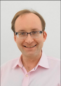
Sergei V. Kalinin is a corporate fellow at the Center for Nanophase Materials Sciences (CNMS) at Oak Ridge National Laboratory. He is also a Joint Associate Professor at the Department of Materials Science and Engineering at the University of Tennessee-Knoxville. Kalinin graduated with M.S. from the Department of Materials Science, Moscow State University, Russia in 1998. He received his Ph.D. in Materials Science and Engineering from the University of Pennsylvania in 2002 under Prof. Dawn Bonnell. He has been a research staff member at ORNL since October 2004 (Senior since 2007, Distinguished since 2013). Previously he was Theme leader for Electronic and Ionic Functionality at CNMS, ORNL (2007– 2015). He was a recipient of the Eugene P. Wigner Fellowship (2002 – 2004). Kalinin’s research focuses on the applications of machine learning and artificial intelligence techniques for the analysis of nanometer-scale and atomically resolved imaging data, with the central concept being the extraction of physics of atomic, molecular, and mesoscale interactions from imaging data and enabling the real-time feedback for controlled matter modification, patterning, and atom by atom fabrication. He is a recipient of the Presidential Early Career Award for Scientists and Engineers (PECASE) in 2009, Blavatnik Award Laureate (2018), IEEE-UFFC Ferroelectrics Young Investigator Award in 2010, Burton medal of Microscopy Society of America in 2010, ISIF Young Investigator Award in 2009, American Vacuum Society 2008 Peter Mark Memorial Award, 2003 Ross Coffin Award and 2009 Robert L. Coble Awards of American Ceramics Society, RMS medal for Scanning Probe Microscopy (2015); 4 R&D100 Awards (2008, 2010, 2016, and 2018) He was named a fellow of Materials Research Society (2017), Foresight Institute (2017), MRS (2016), AVS (2015), APS (2015), and a senior member (2015) and Fellow (2017) of IEEE.

Jeff’s adventures began at D. E. Shaw & Co., in NYC after graduating with his BS & MS in computer science from the University of Illinois, Urbana-Champaign. Jeff Bezos was his first manager, and they worked together for three years before Bezos started Amazon. Jeff moved over to Amazon in 1997 and spent almost 9 years there, first leading the charge on Amazon’s back-end supply chain and fulfillment infrastructure and then heading up Consumer, where he delivered Amazon Prime amongst many other things. After Amazon, Jeff co-founded and served as CEO of Pelago, a startup focused on urban discovery and recommendations based on GPS history. After 5+ years and two successful funding rounds, he sold Pelago to Groupon and joined as SVP, Product. In 2014, he joined Uber as its Chief Product Officer, where he spearheaded Self-Driving (ATG), Eats, Pool, AI Labs, Elevate, and Uber’s developer API. Atomic Machines is a pursuit of passion for Jeff: he is fascinated by the command of matter and looks to bring all of his experience to bear to create a radically innovative and durable company singularly focused on ushering in the era of atomically precise manufacturing.

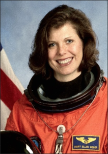
Dr. Mary Ellen Weber was a NASA Astronaut for ten years and is the veteran of two spaceflights, including one to construct the International Space Station. She is currently a consultant on strategy, technology, and high-risk operations through her company, Stellar Strategies, LLC, and has been an advisor to NASA on the Advisory Council Committee for Technology, Innovation, and Engineering since 2012. In addition, for nine years, she was a vice president at UT Southwestern Medical Center, a world-renowned medical school, research powerhouse, and hospital in Dallas, Texas. She holds an M.B.A. from Southern Methodist University, a Ph.D. in chemistry from UC Berkeley, and a B.S. in chemical engineering from Purdue University.

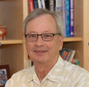
Don worked in nanotechnology research for over 40 years. He retired in 2019 from Cornell University, where he served as Director of Operations for the Cornell NanoScale Science and Technology Facility (CNF) from 2006 – 2019, preceded by a 27-year career at Bell Labs. At Bell Labs, Don was a Distinguished Member of Technical Staff where he managed the Advanced Lithography Group in the Nanofabrication Research Department. He worked in high-resolution electron beam lithography and related nanofabrication technology. His work has had a significant impact on a wide range of disciplines, including soft X-ray imaging, extreme ultraviolet lithography (EUVL), precision optical network components, and technologies for high-performance superconducting and semiconductor devices. He has authored or co-authored hundreds of articles in these fields, organized major international conferences, presented numerous invited technical talks, and has been awarded 11 U.S. patents. Don was long-affiliated with the International Conference of Electron, Ion, and Photon Beams and Nanotechnology (EIPBN), where he served as conference chair, advisory member, and financial trustee. He is a past chairman of the Nanoscale Science and Technology Division of the AVS and was named a Fellow of the AVS in 2010. He was a Scientific Advisory Board member for the Nanoscale Science Research Facilities at Argonne and Lawrence Berkeley National Labs. His most recent effort at Cornell’s CNF was to renew and expand the facility into four strategic areas of technology: chip-based biotechnology; hetero-integration of CMOS with other application-specific materials; device processing on 2D materials; and materials and technologies for quantum information. Since retiring, he loves spending time with his four grandchildren and honing his skills in woodworking and nature photography.