Atomically-Precise Nano-Imprint Lithography: A Brief Story
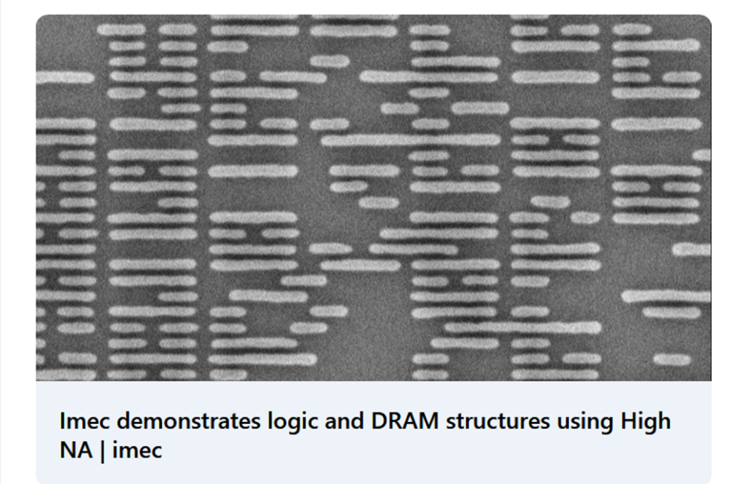
EUV, the current standard for photolithography in the semiconductor industry, is reaching a practical limit of 8 nanometer linewidth, and the cost of the tool is increasing exponentially with each new generation. Speaking of the latest generation, the image below is a demonstration of the resolution of IMEC’s cutting-edge High NA EUV tool, with a 19 nm pitch [1].
We at Zyvex Labs asked ourselves: what’s next? Can we do better? Well, Jet & Flash NanoImprint Lithography (JF-NIL), invented by S.V. Sreenivasan and Grant Wilson at Molecular Imprints (acquired in 2014 by Canon Nanotechnologies) has emerged as a lower-cost, more precise contender that can evolve to a deep single-digit nanometer lithography tool with much lower R&D costs [2].
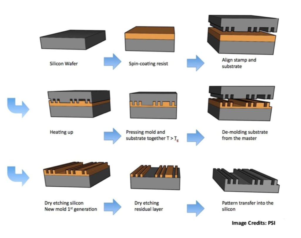
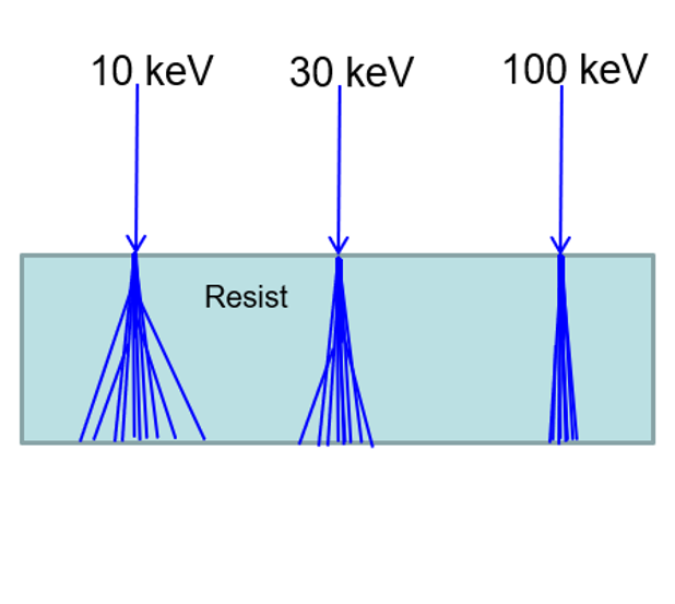
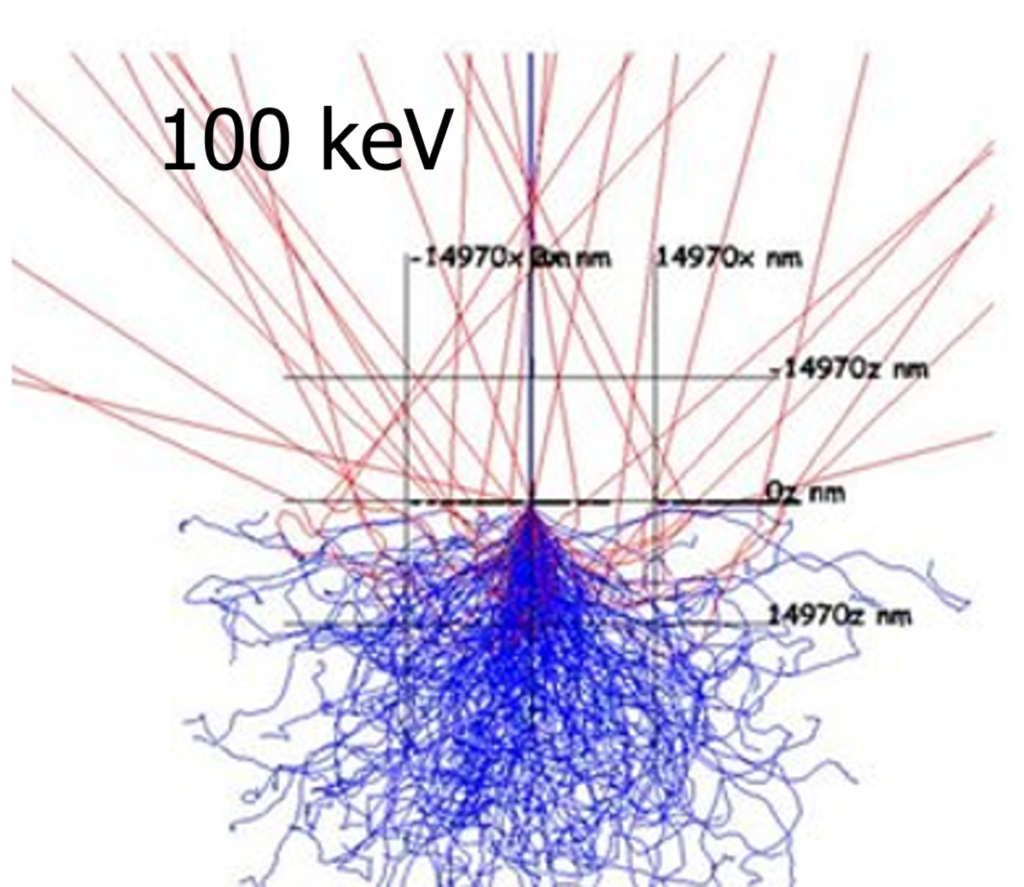
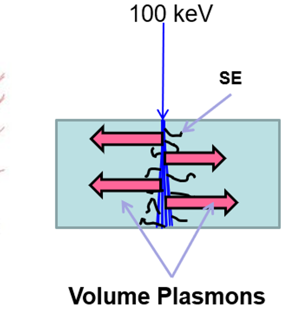
Canon claims a 5 nanometer feature size is possible, but NIL requires a 1-to-1 mask in order to create the actual imprint, so how would we create a 5nm mask? E-beam lithography, the current lithography method of choice for mask-making, has a practical limit of around 15 nm feature size, caused by various factors including (but not limited to) both forward and backward scattering of electrons [3]. This poses a problem for creating masks at such a scale. While isolated lines as small as 4 nm have been demonstrated, a 30 nm pitch (15 nm lines and spaces) is as good as it gets— but it still isn’t good enough.
That’s where atomically-precise STM lithography comes in [4,5]. With our system, we can reach a pixel size of 0.768 nanometers; that’s 2×2 atoms! Furthermore, our atomically-precise lithography is far cheaper and more energy-efficient than the existing alternatives.
In order to convert the original STM pattern to a usable NIL mask, TiO2 is deposited on top of the original pattern in a process called atomic layer deposition (ALD). From there, it is used as an etch mask for Reactive Ion Etching (RIE) to form a 2.5D Si template, replicating the STM pattern [6]. Unfortunately, in practice, some resolution is lost over the course of the process. Despite that, on our very first attempt with this process 10 years ago, we managed to create masks with a feature size of 8-10nm— better than the highest-resolution results achievable by the latest and most expensive EUV and E-Beam lithography systems (making 4-to-1 masks). We plan to continue honing the technology until feature sizes of 5 nanometers are both achievable and financially-accessible.
In October of 2023 [1], Canon Nanotechnologies announced they were entering the semiconductor market with Jet-Flash NIL, aiming to compete with ASML’s EUV scanners. In August of 2024, IMEC released a test pattern demonstrating the capabilities of ASML’s latest high-NA tool for use in logic and DRAM semiconductor applications. Their pattern had a full pitch of 19nm. In September of 2024, we created a replica of the same pattern in STM lithography— except at 40% scale. The pitch was 7.7nm (10 pixels).
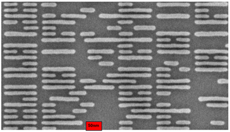
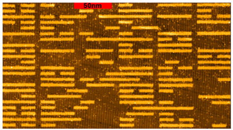
IMEC’s lithography, 19nm pitch (left), vs Zyvex Labs’ initial STM lithography pattern, 7.7nm pitch (right)

As you can see, not only is our pattern smaller, it’s more precise (due to a lack of proximity effects, a downfall of photolithography).
There is, however, another issue: throughput. Tennant’s Law [7] states that throughput scales, not linearly or quadratically with resolution, but with the 5th power of the resolution. So, by using the existing EUV and E-beam methods, if one were to double the resolution of a pattern that took a day to complete, the new version would take a month. Atomically-precise lithography, however, has the advantage of being able to use multiple tips efficiently. The E-beam Multi Beam Mask Write (MBMW) has 262,144 beamlets, but only a throughput increase of 10x [8]. This is due to charged particle interaction between all of the beamlets. However, using MEMS z-actuators for each tip, we can make a multitip atomically-precise lithography tool without those charged particle interactions, thus scaling throughput linearly with the number of tips. This is due to the fact that, in STM lithography, the electrons tunnel directly from each tip to the surface, eliminating charged particle interactions. We believe that the scanning method most suited to a multi-tip array is a technique called ‘raster scanning’, where multiple tips follow the same X-Y path, but the user controls whether any given tip is actively writing. Additionally, in raster lithography, each tip is only responsible for creating the pattern within its own “sector”. Thus, every tip can each make a unique pattern, stitching together with its neighbors. It doesn’t matter how large the pattern is; as long as the array is big enough to accommodate, the write time stays exactly the same.
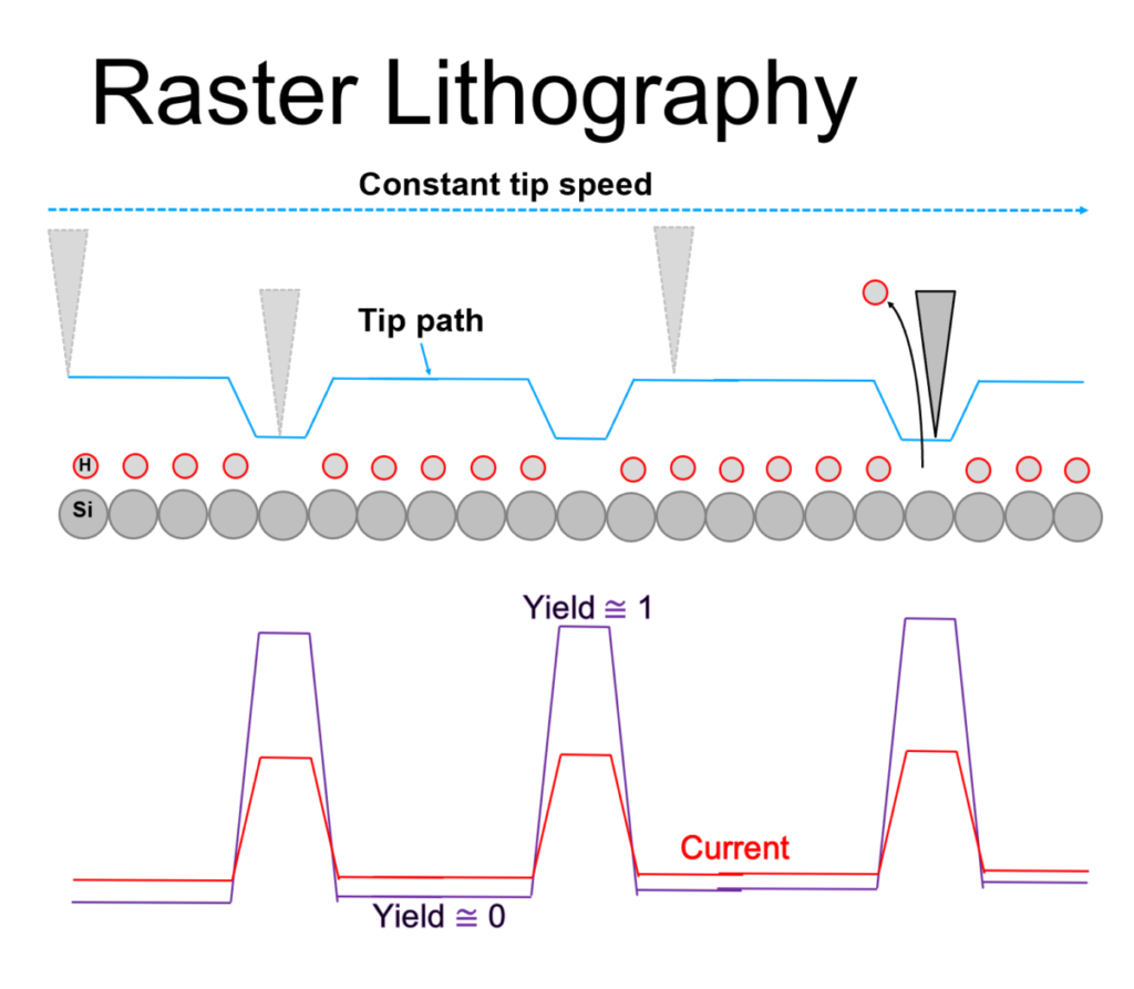
With a raster scanning array of enough tips, we can likely match and exceed current E-beam speeds (including multi-beam mask writers), but with much finer resolution and precision [9]. Due to all the factors mentioned above, atomically-precise nano-imprint lithography stands out as a keystone to the future of lithography technology (as well as the many technologies that currently rely on photolithography for manufacturing).
Bibliography
- https://www.imec-int.com/en/press/imec-demonstrates-logic-and-dram-structures-using-high-na-euv-lithography
- October 13, 2023, Canon announced today the launch of the FPA-1200NZ2C nanoimprint semiconductor manufacturing equipment https://global.canon/en/news/2023/20231013.html
- Determining the resolution limits of electron-beam lithography Manfrinato, V. R., et.al. Nano Letters, 14(8), 4406–4412.
- Atomically precise digital e-beam lithography
J. N. Randall, J. H. Owen, E. Fuchs, R. Saini, R. Santini, and S. O. R. Moheimani, in Novel Patterning Technologies for Semiconductors, MEMS/NEMS and MOEMS 2020, 2020, no. March 2020, p. 31. - Scalable digital atomic precision lithography
E. Fuchs, J. H. G. Owen, A. Alipour, E. L. Fowler, S. O. R. Moheimani, and J. N. Randall, in Novel Patterning Technologies 2023, 2023, p. 22. - Atomically Traceable Nanostructure Fabrication
Ballard, Josh B. and Dick, Don D. and McDonnell, Stephen J. and Bischof, Maia and Fu, Joseph and Owen, James HG and Owen, William R. and Alexander, Justin D. and Jaeger, David L. and Namboodiri, Pradeep and Fuchs, Ehud and Chabal, Yves J. and Wallace, Robert M. and Reidy, Richard and Silver, Richard M. and Randall, John N. and Von Ehr, James
JoVE (Journal of Visualized Experiments) (2015) [doi:10.3791/52900] - Donald M. Tennant, Chapter 4, “Limits of Conventional Lithography”, in Nanotechnology, Gregory Timp Ed., Springer (1999) p. 164.
- Private conversation with CTO of one of the world’s largest mask makers.
- Atomically precise digital e-beam lithography, J. N. Randall, J. H. G. Owen, E. Fuchs, R. Saini, R. Santini, S. O. R. Moheimani, “Atomically precise digital e-beam lithography,” Proc. SPIE 11324, Novel Patterning Technologies for Semiconductors, MEMS/NEMS and MOEMS 2020, 113240X (23 March 2020); doi: 10.1117/12.2552083