DOE SBIR – Epitaxy
For 3D quantum devices, we need to be able to place atomically-precise patterns above buried patterns. To do this, the surface roughness after the low-temperature epitaxy needs to be much improved. We will explore ways to improve the epitaxial overgrowth, and to demonstrate alignment of a dopant pattern to a buried dopant structure.
DOE – AQS for Nuclear Physics
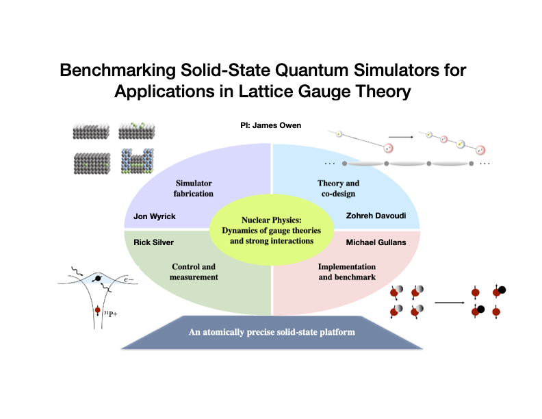
In this speculative program, we aim to answer the question, “Can Analog Quantum Simulators help solve real problems in Nuclear Physics?”. In particular, we will create dopant-based AQS devices using STM-based lithography to create an experimental implementation of the rotor Rabi-Jackiw model.
DOE AMO STTR Phase I & Phase II “BJTs”
By using STM based Hydrogen Depassivation Lithography (HDL) and dosing with both acceptor and donor precursors to make bipolar delta-layers (all dopant atoms in a single buried (100) atomic plane. In this way we can make 2D Bipolar Junction transistors that are expected to have an extremely high gain bandwidth ratio, be extremely low-noise, have unprecedented control of device performance properties, operate at cryogenic temperatures, and be extremely rad-hard.
Atomically Precise Ultra-High Performance 2D Micro Electronics
- Collaborators:
- 3-D Epitaxial Technologies – Wylie Kirk
- Sandia National Labs – Shashank Misra

DOE AMO STTR Phase I & Phase II “Dopants”
The overall objective of this program is to improve the metrology of buried dopant structures for ultraprecise devices created using Scanning Tunnelling Microscope (STM) based lithography. During fabrication, it is necessary to determine the location of existing structures so as to align new dopant structures to them precisely. This metrology therefore needs to be done in-situ during fabrication with the same probe as used for lithography Second, for quantum devices, it is proving more important that there be the desired number of dopants in a patch, rather than that their position is atomically precise. In-situ metrology allows the possibility of error correction. This is a hallmark of Atomic Precision Advanced Manufacturing.
Atomically Precise Scanning Probe Based Analysis of Activated Dopants for 2D Micro Electronics
- Collaborator
- University of Texas at Dallas – Reza Moheimani
DOE BES STTR Phase I & Phase II
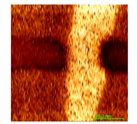
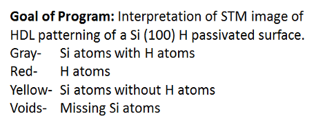
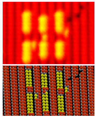
The goal of the program is to have image analysis routines that can make decisions allowing automated routines to proceed efficiently without human intervention. If successful this will be an important step to Atomically Precise manufacturing. The figure suggests what we expect to accomplish: Take a moderate quality STM image and determine unambiguously where all of the atoms are on the surface.
STM based Hydrogen Depassivation Lithography Automation Via Artificial Intelligence
- Collaborator
- Oak Ridge National Labs – Sergei Kalinin & Maxim Ziatdinov
DARPA DSO STTR Phase I
Products for Fabrication of Atomically Precise Strongly Correlated Materials
- Collaborators:
- 3-D Epitaxial Technologies – Wiley Kirk
- University of Washington at St. Louis – Erik Henricksen & Kater Murch
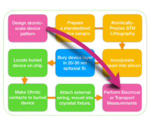
By supplying a suite of sample, fabrication, and measurement products, the dopant-in-Si approach will make Fermi-Hubbard physics research far more accessible to a broader range of researchers.
DOE AMO STTR Phase I, Phase II, & Phase IIB
The goal of the STTR program is to commercialize MEMS based STM scanners starting with a Z-axis only Single tip and progressing to 3-Axis MEMS that could replace piezo tube scanners in STMs and then make arrays of XYZ scanners for HDL tools. Research suggests that massively parallel arrays are feasible, leading the way to HDL manufacturing tools.
High Speed Platform for APM and Hierarchical Assembly
- Collaborations
- University of Texas at Dallas – Reza Moheimani
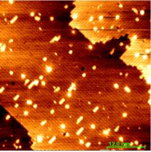
DOE 1465 Atomically Precise Manufacturing Program
A Platform Technology for High-throughput APM Mechatronics at the Atomic Scale
The goal is automated, parallel, Atomically- Precise HDL manufacturing tools. Multiple designs of MEMS actuators, realizing both AFM for rapid sample surveys, and STMs for precision imaging and lithography are being designed, built and tested. Advanced control systems and multiple modes of operations are being explored for use in pipelined HDL exposure processes.
- Collaborators:
- University of Texas at Dallas – Reza Moheimani (Prime)
- National Institute of Standards and Technology – Jason Gorman
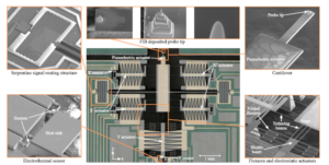
DOE 1465 Atomically Precise Manufacturing Program
2D materials have unique electronic properties that can be exploited in a wide variety of manners. However, there are only a limited number of 2D materials currently known and each has its own unique properties that may or may not fit well to a particular application and new material systems are extremely expensive to develop. Atomically Precise Manufacturing can enable the creation of designed 2D materials that will allow specific electronic properties to be obtained in silicon, a very well established material system. This can be accomplished by the atomic precision placement of dopant atoms in a single atomic plane of silicon buried beneath the surface.
- Atomically Precise Manufacturing for 2D-Designed Materials
- Program Collaborators:
- National Institute of Standards and Technology – Richard Silver
- 3-D Epitaxial Technologies – Wylie Kirk
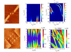
DARPA Tip-Based Nanomanufacturing Program
In this program we made significant strides towards developing a tip based patterning technique and associated pattern transfer technology that will enable atomic precision and then absolute precision for both specific manufacturing and foundry services to a wide variety of nanotechnology products and applications.
- Atomically Precise Manufacturing
- Program Collaborators:
- University of Texas at Dallas – Yves Chabal, Bob Wallace, K.J. Cho
- University of Illinois at Urbana-Champaign – Joe Lyding
- University of Texas at Austin – S.V. Srinivasan
- University of North Texas – Rick Reidy
- University of Central Florida – Dennis Deppe
- National Institute of Standards and Technology – Richard Silver
- Integrated Circuit Scanned Probe Instruments, Inc. Systine, Inc. – Stewart Sando
- Molecular Imprints, Inc. – S.V. Srinivasan
- Vought Aircraft – Martin Wimmer
- General Dynamics A.I.S. – Tihamer Toth-Fejel

ARO Silicon Quantum Computing Program
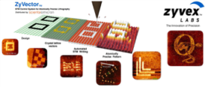
This program essentially paid for the development of the ZyVector™ product and placed units at Sandia National Laboratory and the University of New South Wales in Australia.
- Atomic Precise Fabrication for Qubit Devices
- Collaborating Institutions:
- Sandia National Labs – Shashank Misra
- University of Texas at Dallas – Reza Moheimani
- University of New South Wales – Michelle Simmons
- University of Maryland – Chris Richardson
- Systine, Inc.
DARPA Atoms to Products (A2) Program
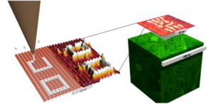
Aiming to scale up atomic-scale devices to µm-scale collections of devices, which would in turn be scaled up to mm-scale devices.
- Atomic Manufacturing, Micron Assembly, Zyvex Engineering
- Program Collaborators:
- University of Texas at Austin – S.V. Srinivasan
- University of Texas at Dallas – Reza Moheimani
- Rice University – Naomi Halas
- Systine, Inc. – Stewart Sando
- SRI, Inc. – Ron Pelrine
- Integrated Circuit Scanned Probe Instruments, Inc. – Neil Sarkar
- National Institute of Standards and Technology – Richard Silver
NSF GOALI Program
Nanomanufacturing of acceptors for atomically precise 2D bipolar devices
Collaboration with 3-D Epitaxial Technologies
Additional Collaborating Institutions
University College London – David Bowler & Neal Curson
University of New Mexico – Tito Bussani
University of Chicago – Giulia Galli & David Schuster