
←2012 |
2014→ |
MNE 2013 Micro Nano Graph Contest
“ A good Micrograph is worth more than the MegaByte it consumes.”Entries Presented by Dr. John Randall – Zyvex Labs Sponsored by
The rules include the following:
• Entries have to be of a single image taken with a microscope and not significantly altered.
• There is no restriction with respect to the subject matter.
• Electron and ion micrographs have to be black and white.
In 2013, 62 entries were submitted from 11 countries. There were many outstanding micrographs. The work represented in the submitted micrographs covered a wide range of fields including micro mechanical, photonic, and integrated circuit fabrication, chemical and dry etching, biological samples, material science experiments and, of course, e-beam, ion beam, and nano imprint lithography experiments.
The panel of judges who selected the award winners were:
- Larry Millstein – USA
• Steven Schofield – UK
• Massimo Gentili – Italy
The Awards are:
• First Prize
• Second Prize
• Third Prize
The judges also selected 4 Honorable Mentions.
All 2013 Entries (with original titles)
Judges exercised their prerogative to change the micrograph titles if it pleased them.
First Prize
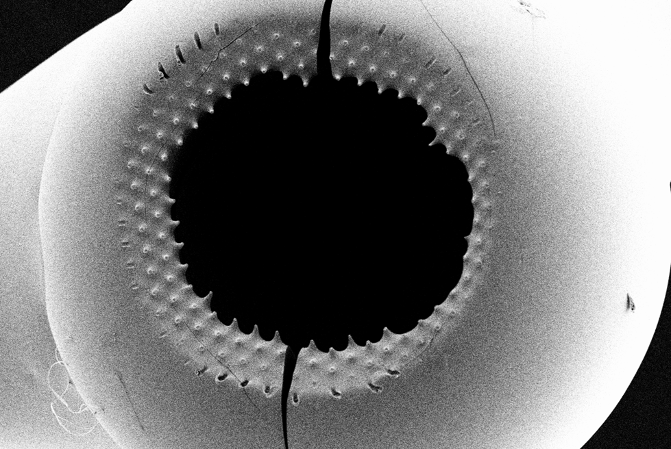
Title: “The Micro Pit of Carkoon”
Description:
Lysozyme residual coming from droplet drying on a micropillar superhydrophobic substrate. The protrusions are due to the pinning effect of the droplet on the microasperities of the surface.
Spatial monster or black hole, it is better to run!!!
Magnification (3″x4″ image): 497X
Instrument: FEI Helios Nanolab 600
Submitted by: Angelo Accardo
Affiliation: Italian Institute of Technology, Genova, Italy
Second Prize
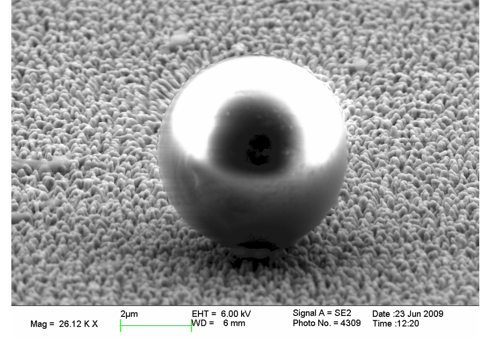
Title: “Charged UP”
Description:
This is an image of an artefact. We don’t know what it is. Only that it could move by scanning it. Interestingly you can see the detector in the reflection.
Magnification (3″x4″ image): 26KX
Instrument: Leo 1550
Submitted by: Michael Schmidt
Affiliation: Dept. Micro- and Nanotechnology, Technical University of Denmark
Third Prize
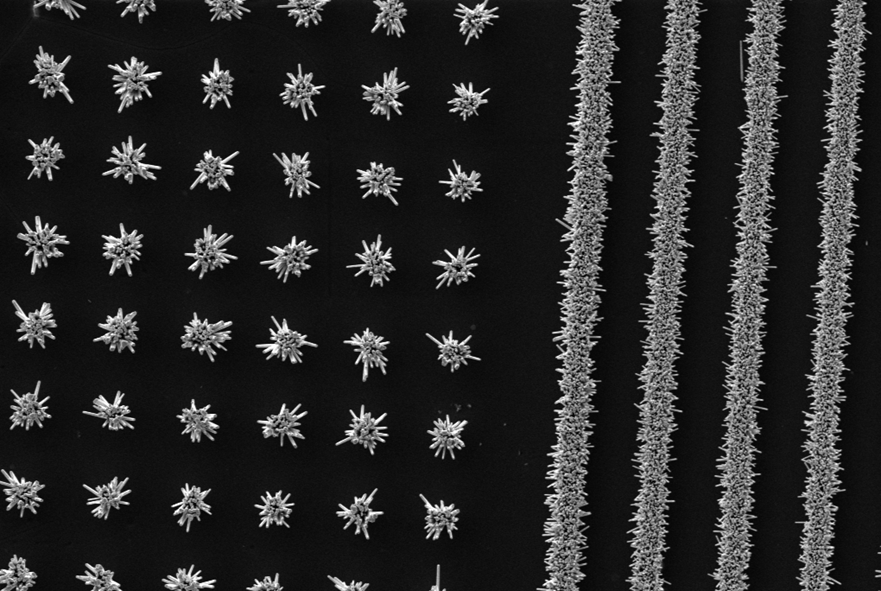
Title: “Stars and Stripes”
Description:
NWs bunch and stripes growth by hydrothermal technique. The growth is driven by a patterned resist layer on a ZnO(30nm)/Si substrate. The image is acquired with 45° tilt.
Magnification (3″x4″ image): 2.7KX
Instrument: zeiss EVO MA10
Submitted by: Marialilia Pea
Affiliation: Institute of Photonic and Nanotechnology, Rome, Italy
Honorable Mention
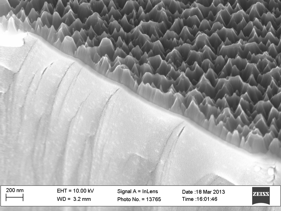
Title: “Waterfall”
Description:
Nanoforest on SiC substrate. The waterfall is due to damaged edge of the sample.
Magnification (3″x4″ image): 25KX
Instrument: Zeiss Supra VP 40 SEM
Submitted by: Aikaterini Argyraki
Affiliation: Technical University of Denmark, DTU
Honorable Mention
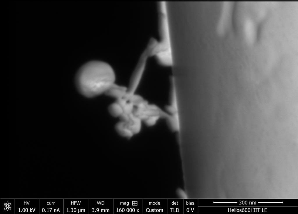
Title: “Nano Climber with Son”
Description:
Beyond the nanoworld there is a lady climbing a tapered optical fiber in order to save her baby (attached to her backpacking) from the fire emitted from the fiber tip.
This stunning defect arose after having melted the gold coating of a tapered optical fiber with a too high power of the guided light.
Magnification (3″x4″ image): 160 KX
Instrument: Elios600i
Submitted by: Ferruccio Pisanello and Leonardo Sileo.
Affiliation: Italian Institute of Technilogy, Center for Biomolecular Nanotechnology, Lecce, Italy
Honorable Mention
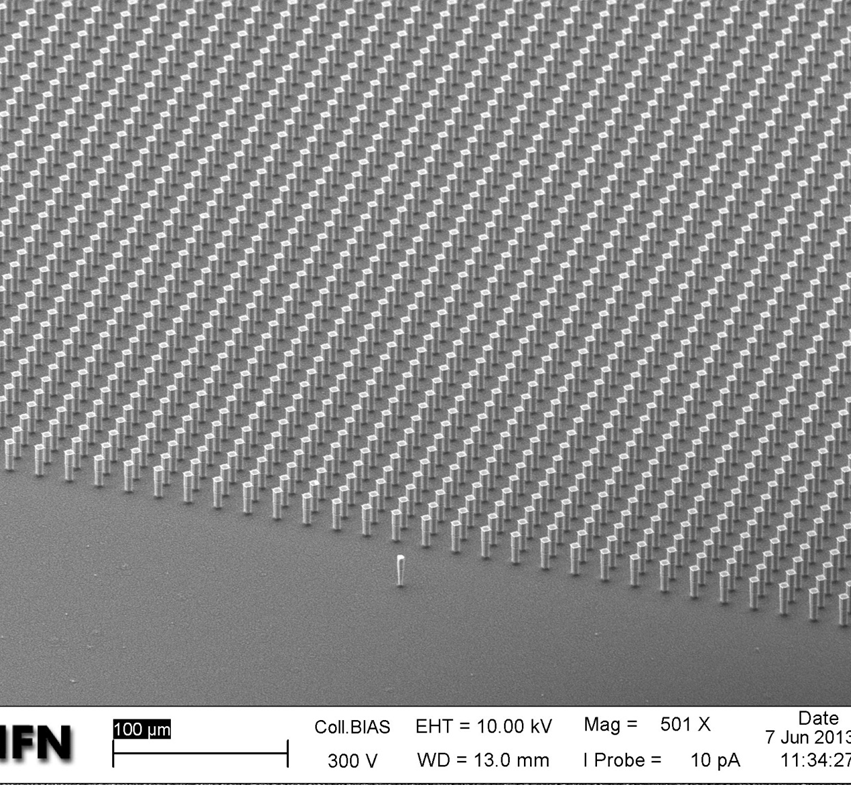
Title: “The Pledge”
Description:
Superhydrophobic structure made of silicon pillars 3 microns in diameter, 20 microns heigth, 20 microns period. ICP Bosch process
Magnification (3″x4″ image): 500X
Instrument: Zeiss EVO MA10
Submitted by: Luca Businaro
Affiliation: CNR – Institute for Photonics and Nanotechnologies, Rome Italy
Honorable Mention
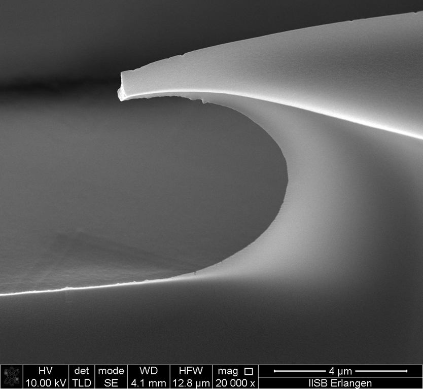
Title: “Microwave”
Description:
Wave-like feature formed due to the incomplete filling of the mold structure during an imprint.
Has anyone seen the Silver Surfer?
Magnification (3″x4″ image): 20KX
Instrument: FEI Helios Nanolab 600
Submitted by: Maximilian Rumler
Affiliation: Fraunhofer IISB Erlangen